


VISION*
Yotta's domain experience spans the semiconductor ecosystem from the creation and development (circ. 1982) of some of the industry's leading manufacturing technology, Atomic Layer Deposition and Etch (ALD and ALE), to the creation and development (circ. 2002) of some of the industry's leading design methodology infrastructure, OASIS. Both had taken a decade or more to become mainstream. Today, ALD and ALE have become gating factors driving the successes of advanced semiconductor technology. OASIS is in use from Standard Cell library development through tapeout / the entire process development to design to manufacturing workflow / from ideas to devices.
There is a great deal of uncertainty at the leading edge of semiconductor technology. Opportunities to consolidate, as the industry has in the past, are gone. Atypical collaborations and alliances are forming (e.g. GlobalFoundries and Samsung / Intel and TSMC / Altera and Intel / Oracle, Sun, Fujitsu and TSMC / Apple, Samsung and TSMC). System OEMs are bypassing Fabless companies. They're looking for a direct a connection to the Foundries. Both are sitting on the fence or defecting / both with very short-term outlooks on their relationships with the Foundries / the risks and costs to scale to next generation technology too high to go it alone / the addressable markets justifying new technology not fully understood but known to be of the size of humanity's deeper challenges.
The successes of the solutions to humanity's deeper challenges will depend on advances in semiconductor technology. The semiconductor industry has evolved from being foundry-centric to a single, heavily siloed and largely inefficient, $315B IDM - the very model that had forced the IDMs of the past to make a move to a Foundry business model. What can be done this time that keeps this IDM's technological risks and costs scaling well with the development of its new addressable market, namely humanity? Other than through partnerships, acquisitions and joint ventures ('collaborations'), there isn't anything that can be done. The workflow has been hardwired for 25 years.
Perhaps industry wide collaborations, etc. will be enough for 14nm and perhaps even 10nm. Whether 10 nm being the limit, history has shown that a fully idealized IDM business model (e.g. Intel) will not be enough to resolve tomorrow's sub-10 nm era technological challenges. The industry at the leading edge will need an unprecedented depth of focus into the ecosystem wide data they have before them / an unprecedented (single) clarity of view of their process-to-design-to-manufacturing workflow / one that resolves to the finest level of meaningful detail that has been squeezed into a byte of data / a developing (dynamically referential and archival) view of every meaningful thought that had led to the current state of semiconductor design and manufacturing technology.
The semiconductor industry and its constituents are at yet another point in time where they're being forced to make some tough decisions about how to advance semiconductor technology and meet the needs of its projected addressable markets. What is the industry's and the industry's stakeholders' core business? What will be the new competitive differentiators? ICs at 10 and 7nm technology? Or, will it be what we can do with such a capability? Solutions for humanity? Some in the industry believe their future to be the latter. Because the industry has become one large IDM and its addressable market humanity, should tomorrow's business (humanity's deeper, and much larger and more comprehensive, challenges) be addressed collaboratively? Cisco, Intel, AT&T and General Electric think so. To place this future Collaborative Commons in perspective. The combined revenue for the four companies ($316B) is the same as the revenue generated by the entire semiconductor industry. If the rest of the semiconductor industry can do the same, its constituents can let go of advances in semiconductor technology as their differentiator. They'd be able to collaboratively drive advances in semiconductor technology into the sub-10nm era with this deeper level view of the developing information within its workflow. Everyone will be more informed and, thus, empowered to advance semiconductor technology. They'll be able to reduce the costs and risks and have a new, longer-term, differentiator. The differentiator of the future being what the industry and its customers do for humanity with those 10 and 7nm chips.
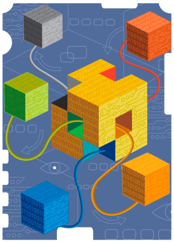
Yotta believes that the next effort by the semiconductor industry will be to consolidate common interests by the clarification and sharing of what it knows at the leading edge of semiconductor technology. This path has been the path the industry has taken for decades, the last being industry's move to the Foundry and 3rd Party IP business models. The difference this time is the size of the effort; an entire industry working toward but a few common technological objectives.

Samsung was about better displays, better TVs and better phones. The question I think is, where do we go from here to innovate that are software that are cloud that are more bio and the more interdisciplinary type of opportunities that can help us (society) to grow? We need to be able to contribute to better living. I think that era of using data to help us live better is coming. It’s about Big Data; Big Data to help us to grow and make sense out of what we do. So, I see that as a huge potential opportunity.
Young Sohn
President and Chief Strategy Officer
Samsung Electronics
December 2013
With each generation of semiconductor technology, more of our lives have been virtualized. We've developed an understanding that we can "map" the brain and mind. Billions of dollars have been committed to doing so. We're of the belief that we can reach for and have economic, social and ecologic sustainability.
Advances in semiconductor and embedded technology will take us there.

Integrated Device Manufacturer (IDM)
Manufacturing (M)
Equipment and Facilities
CAD
Assembly / Test
Deposition
Etch
Lithography
Metrology
Mask
Design
Design
Manufacturing
Assembly / Test
Foundry
Deposition
Etch
Lithography
EDA
Metrology
Mask
$317B (2013) IDM
Manufacturing
Intel, Samsung, TSMC
Equipment and Facilities
Synopsys
ASE
Applied Materials
Lam Research
ASML
KLA-Tencor
NuFlare, Dai Nippon Printing
Design
Apple, Qualcomm, ARM
2014
Peak of Consolidation
Apple / TSMC / Samsung
Samsung / GlobalFoundries
Qualcomm / TSMC / SMIC
2013
Altera / Intel
2011
Oracle/Sun Microsystems
2009
Intel / TSMC
AMD / GlobalFoundries
1990
ARM Holdings
1987
TSMC
1967
Consolidation of Shared Interests
Applied Materials
Commercialization of the Semiconductor Workflow
1957
Growth
Fairchild Semiconductor
First IDM Business Model
Internally Developed Workflow
Fujitsu wants to create a new type of society, where people’s lives are enriched by Information and communication Technology (ICT) and innovation is everywhere, delivering new business and social value. Fujitsu calls this a Human Centric Intelligent Society. Getting there is our goal.
Fujitsu Technology and Service Vision
March 2013
It is a high-risk, high-reward environment. If foundry/fabless companies establish an IDM-type interface, there is no reason that they cannot be as effective as an IDM.
EETimes
June 15, 2012
Last October, GE (NYSE:GE) announced a partnership with Intel (NYSE:INTC), AT&T (NYSE:T), and Cisco to introduce 14 new Internet-connected industrial products to clients in the aviation, power, water, transportation, oil and gas, health care, and energy management industries.
CIO Magazine
March 2014.
OAS = OASIS
GDS = GDSII
Workflow Auditor Point Tools
TM
®
© Getty Images
NEW at Yotta Data Sciences
* US Patents 9,122,825, 8,555,219, 8,266,571 and 7,685,545.
International Patents: China 200980129771.8, Japan 4768896, Korea 10-1580258, Israel 209907, European Patent 2310967.
OASIS® is a Registered Trademark of Thomas Grebinski
© 2008-2022 Yotta Data Sciences, Inc. All rights reserved.
OASIS® is a Registered Trademark of Thomas Grebinski
© 2008-2024 Yotta Data Sciences, Inc. All rights reserved.
February 16, 2024- Yotta is offering, to qualified partners, a six-month evaluation-period, with support, for its SEMI P39-0416 OASIS Reader/Writer Source Code.
Visit Page: OAS Reader/Writer
Visit Page: OAS Source Code