SAMPLE 20 and 14 nm CPU PLANAR STRESS TEST CASES
14 nm Processor Core
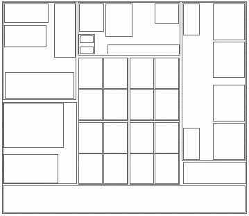
A version of the 14 nm demonstration synthetic design/stress test case is available for download now at the Yotta FTP site. This is a small processor core, similar to an ARM processor. It is 340.4 microns wide and 295.5 microns high. The full GDSII file is about 1,038.2 megabytes in size and the full OASIS file is about 60.8 megabytes in size.
The processor core includes 16 kilobytes of level 1 cache SRAM; there are also small memory blocks for register files. Altogether there are 379,264 bits of SRAM including ECC. After expanding all design hierarchy, there are 376,615 placed standard cell instances and 5,446,450 transistors.
The design rules are aggressive (14 nm width, 14 nm spacing, no enclosure around contacts or vias) to stress capacity limits and provide as many regions of 28 nm pitch as possible. The layout of an SRAM bit cell does not provide many places where minimum single‐layer spacings apply, so most of the minimum pitch areas are in the standard cell routing.
Layer definitions are available in the 14 nm Processor Core Data Sheet.20 nm Processor Core
20 nm Processor Core
A version of the 20 nm demonstration synthetic design/stress test case is available for
download now at the Yotta FTP site. These are small processor cores, similar to an ARM
processor. It is 487.2 microns wide and 422.4 microns high. The full GDSII file is about 622.5 megabytes in size and the full OASIS file is about 37.1 megabytes in size.
This demonstration design file is meant to show the cell generation, placement and routing and floor planning capabilities of the Yotta Data Sciences synthetic design/stress test case generator. The processor core in it is part of Yotta’s IP library; it is placed 26 times in version 2 of the 20 nm network processing SoC stress test case.
The processor core includes 16 kilobytes of level 1 cache SRAM; there are also small memory blocks for register files. Altogether there are 305,536 bits of SRAM including ECC. After expanding all design hierarchy, there are 210,305 placed standard cell instances and 3,734,176 transistors.
Layer definitions are available in the 20 nm Processor Core Data Sheet.
Sample 20 and 14 nm Planar Layout Stress Test Case Download Request
Sample 20 and 14 nm Planar Layout Stress Test Case Data Sheet Request
 | ||||
"The Company's technology established a common expectation amongst suppliers and customers regarding matters of OASIS compliance, performance and interoperability"
Naoya Hayashi
Electronic Device Laboratory
Dai Nippon Printing Co., Ltd
typedef struct _oasisReaderPath {
oasisUInt layer,dataType,halfWidth;
oasisInt startExt,endExt;
rawPointList *ptList;
oasisPropertyList *propList;
} oasisReaderPath;
OAS = OASIS
GDS = GDSII
Workflow Auditor Point Tools
TM
®
© Getty Images
NEW at Yotta Data Sciences
* US Patents 9,122,825, 8,555,219, 8,266,571 and 7,685,545.
International Patents: China 200980129771.8, Japan 4768896, Korea 10-1580258, Israel 209907, European Patent 2310967.
OASIS® is a Registered Trademark of Thomas Grebinski
© 2008-2024 Yotta Data Sciences, Inc. All rights reserved.
February 16, 2024- Yotta is offering, to qualified partners, a six-month evaluation-period, with support, for its SEMI P39-0416 OASIS Reader/Writer Source Code.
Visit Page: OAS Reader/Writer
Visit Page: OAS Source Code


