PLANAR LAYOUT STRESS TEST CASES

Yotta Data Sciences has developed a set of IC design stress test cases that will allow developers of physical verification and IC production tools to ensure that their tools will handle the designs of tomorrow. The designs are arbitrarily complex and can be drawn at any desired process node, such as 20 nm, 14 nm, 10 nm, or 7 nm. Custom designs can be created with custom design rules and/or floorplans.
Currently there are eight stress test cases using 20 nm and 14 nm design rules, emphasizing differing styles that will be seen in tomorrow's complex semiconductor design and manufacturing flows. These are not simply repeated blocks of random polygons. They use realistic design rules and leaf cells, with simulated routing and floorplans that resemble real integrated circuits.
These test cases include commercial SRAMs, CPUs, and large SoCs such as Smart Phones, Network Processors and hybrid laptop/tablet computers. The 14 nm designs include a pair that simulate two different IP usage scenarios - all soft IP vs. all hard IP.
The stress test cases feature:
- SRAM blocks using a 6-, 8-, or 10-transistor core cell
- regions of standard cells, placed and routed with multiple metal layers
- simulated processor cores with functional units and cache memories
- top-level routing and power buses
- realistic floorplans with multiple levels of hierarchy
- pad rings
- metal fill
- polygon coloring for multi-patterning
- data volume in line with typical designs at each process node
- polygons colored for double patterning on gate, contact, and metal layers
Preliminary versions of these designs are now available for evaluation; contact Yotta for more information.


 | ||||
"The Company's technology established a common expectation amongst suppliers and customers regarding matters of OASIS compliance, performance and interoperability"
Naoya Hayashi
Electronic Device Laboratory
Dai Nippon Printing Co., Ltd

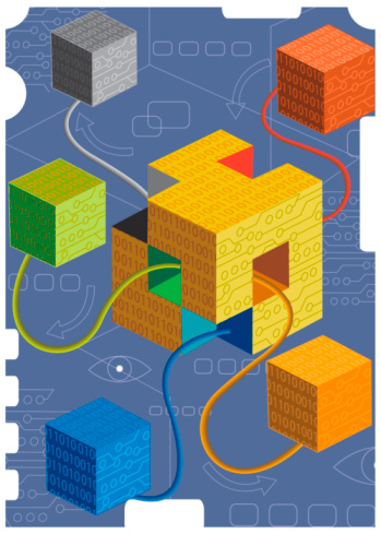

Planar Layout Stress Test Cases
20 nm
14 nm
Each generation of semiconductor technology has enabled the realization of integrated circuits having far more functionality and complexity per square centimeter of silicon. Their realization has required advances in design and manufacturing automation / automation that can virtualize what a next generation integrated circuit may look like and how they'll behave; a developing capability that, decades long, has been defining the leading edge of software and hardware platform computational, memory and storage technology.
Without realistic design and manufacturing data that anticipates the functionality and the complexity of next generation integrated circuits, software and hardware developers have found it exceedingly difficult to produce automation they're confident will meet their customer's needs.
typedef struct _oasisReaderPath {
oasisUInt layer,dataType,halfWidth;
oasisInt startExt,endExt;
rawPointList *ptList;
oasisPropertyList *propList;
} oasisReaderPath;
Click . . . and go.
OAS = OASIS
GDS = GDSII
Workflow Auditor Point Tools
TM
®
© Getty Images
NEW at Yotta Data Sciences
* US Patents 9,122,825, 8,555,219, 8,266,571 and 7,685,545.
International Patents: China 200980129771.8, Japan 4768896, Korea 10-1580258, Israel 209907, European Patent 2310967.
OASIS® is a Registered Trademark of Thomas Grebinski
© 2008-2024 Yotta Data Sciences, Inc. All rights reserved.
February 16, 2024- Yotta is offering, to qualified partners, a six-month evaluation-period, with support, for its SEMI P39-0416 OASIS Reader/Writer Source Code.
Visit Page: OAS Reader/Writer
Visit Page: OAS Source Code