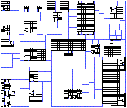
SIMULATED 14 nm SoC (SOFT IP) STRESS TEST CASE

This 14 nm design simulates a complex System-on-Chip (SoC). It is 12495.6 microns wide and 10560.5 microns high and, after expanding all hierarchy, features:
- 14 nm gate length, 28 nm metal pitch;
- 19 small processor cores;
- 7 medium processor cores;
- 10 large processor cores;
- 533,290,995 standard cell placements;
- 651,322,144 bits in all SRAMs; and
- 8,437,111,860 transistors in all circuits.
Not including cache memories within the processor cores, there is 76.5 MB of SRAM with ECC in the design.
The design uses very little “hard IP,” meaning that any licensed design components come in the form of Register Transfer Level (RTL) logic and the customer must run logic synthesis, then place and route on all of the data. The only pre-defined blocks used in this design are three different sizes of processor core, each similar to an ARM processor, plus static RAM (SRAM) in blocks of 128 KB or 512 KB.
It represents one extreme of design philosophy: design blocks should be optimized for a specific design, even if those blocks cannot be used directly in another design. The alternative is to create (or license) validated layout blocks – “hard IP” – and use them in multiple designs. The simulated SoC design using mostly hard IP represents the other extreme, where as much of the design as possible is pre-defined blocks; see our 14 nm hard IP SoC design.
This test case includes two OASIS files, generated using different repetition analysis strategies:
- Type 4-7 (1-D irregular vector) and 10-11 repetitions;
- all orthogonal repetition types (1-7, 10-11) with medium analysis effort.
The preliminary version of the GDSII file is about 301 gigabytes and each copy of the OASIS file is about 18 gigabytes.
With many large blocks (up to eight million placed instances) at the top level of the hierarchy and a GDSII file 300 gigabytes in size, this design will stress your memory and file management code.


 | ||||
"The Company's technology established a common expectation amongst suppliers and customers regarding matters of OASIS compliance, performance and interoperability"
Naoya Hayashi
Electronic Device Laboratory
Dai Nippon Printing Co., Ltd

typedef struct _oasisReaderPath {
oasisUInt layer,dataType,halfWidth;
oasisInt startExt,endExt;
rawPointList *ptList;
oasisPropertyList *propList;
} oasisReaderPath;
Production 14 nm Planar SoC Soft IP Stress Test Case Data Sheet
Sample 20 ands 14 nm Planar Layout Stress Test Cases
OAS = OASIS
GDS = GDSII
Workflow Auditor Point Tools
TM
®
© Getty Images
NEW at Yotta Data Sciences
* US Patents 9,122,825, 8,555,219, 8,266,571 and 7,685,545.
International Patents: China 200980129771.8, Japan 4768896, Korea 10-1580258, Israel 209907, European Patent 2310967.
OASIS® is a Registered Trademark of Thomas Grebinski
© 2008-2024 Yotta Data Sciences, Inc. All rights reserved.
February 16, 2024- Yotta is offering, to qualified partners, a six-month evaluation-period, with support, for its SEMI P39-0416 OASIS Reader/Writer Source Code.
Visit Page: OAS Reader/Writer
Visit Page: OAS Source Code