14 nm 8-CORE finFET MERCHANT CPU STRESS TEST CASE
NO VARIANTS

A preliminary version of a 14 nm finFET eight-core commercial CPU synthetic design/stress test case is available for download now on the Yotta FTP site. This is intended to be similar to a high-end Intel or AMD processor chip.
- 18 nm drawn gate length
- 128 nm SRAM contacted gate pitch
- 130 nm by 600 nm single-port SRAM core bit cell size
- 130 nm by 920 nm two-port SRAM core bit cell size
- 192 nm by 1240 nm three-port SRAM core bit cell size
- two layers of local interconnect
- six layers of metal
- 20 nm fin pitch
- self-aligned double patterning (SADP) for fins
- 1-D gate layer
- 2-D routing
Each processor core has 3-port SRAM for the level 1 cache and register blocks, plus 2-port SRAM for the level 2 cache. Additionally, there is 1-port level 3 cache SRAM around the perimeter of the die. The overall design is about 12,212.7 microns wide and 11,319.6 microns high.
The family of 14 nm finFET design rules used for this design has an 18 nm drawn gate length, a 64 nm theoretical contacted gate pitch, one layer of local interconnect, six metal layers, 64 nm routing pitches for lower metal layers, and 84 nm routing pitches for upper metal layers (metal 4 and up).
All transistor gates are vertical; only gate layer routing within standard cells or SRAM circuits can be horizontal.
Design rule variants in this family can have 1-D routing on any subset of gate or routing layers (except metal 1), or diffraction gratings with blockage or cut masks on any subset of gate or routing layers. Contact Yotta Data Sciences for more information or to request a demonstration file using a particular variant.


Production 14 nm finFET 8-Core (0000) Merchant CPU Test Case Data Sheet
 | ||||
"The Company's technology established a common expectation amongst suppliers and customers regarding matters of OASIS compliance, performance and interoperability"
Naoya Hayashi
Electronic Device Laboratory
Dai Nippon Printing Co., Ltd

typedef struct _oasisReaderPath {
oasisUInt layer,dataType,halfWidth;
oasisInt startExt,endExt;
rawPointList *ptList;
oasisPropertyList *propList;
} oasisReaderPath;
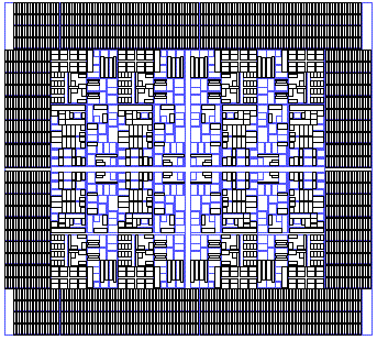
Sample finFET Design Test Cases
OAS = OASIS
GDS = GDSII
Workflow Auditor Point Tools
{0|1} = Cut Mask
{0|1} = Blockage Mask
{0|1} = Diffraction Grating
{0|1} = Fin Pitch Doubling
0 = Not a variant
1 = Variant
| = or
®
TM
© Getty Images
NEW at Yotta Data Sciences
* US Patents 9,122,825, 8,555,219, 8,266,571 and 7,685,545.
International Patents: China 200980129771.8, Japan 4768896, Korea 10-1580258, Israel 209907, European Patent 2310967.
OASIS® is a Registered Trademark of Thomas Grebinski
© 2008-2024 Yotta Data Sciences, Inc. All rights reserved.
February 16, 2024- Yotta is offering, to qualified partners, a six-month evaluation-period, with support, for its SEMI P39-0416 OASIS Reader/Writer Source Code.
Visit Page: OAS Reader/Writer
Visit Page: OAS Source Code