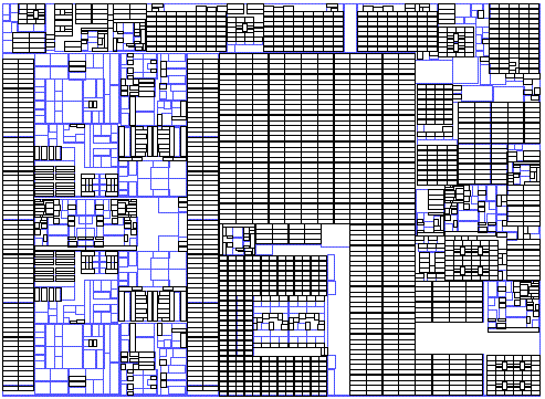
SIMULATED 14 nm SoC (HARD IP) STRESS TEST CASE

This 14 nm design simulates a complex System on Chip (SoC) such as a hybrid laptop/tablet computer chip. It is 6971.0 microns wide and 5086.8 microns high, and after expanding all hierarchy, features:
- 3 small 32-bit processor cores
- 2 medium 32-bit processor cores
- 4 large 32-bit processor cores
- 2 high-speed 64-bit processor cores (from the 14 nm merchant CPU)
- 1 small DSP processor core
- 2 medium DSP processor cores
- 15 large DSP processor cores
- 4 small 8-bit processor cores
- 5 small 16-bit processor cores
- 75,289,255 standard cell placements
- 435,721,280 bits in all SRAMs
- 3,305,650,396 transistors in all circuits
Including cache memories within the processor cores, buffers, and ECC, there is almost 52 MB of SRAM in this design.
This design is nearly all "hard IP," meaning GDSII or OASIS blocks that are licensed from IP vendors and placed in the design without modification.
It represents one extreme of design philosophy: as much as possible, validated design blocks should be licensed from outside specialists. Because IP vendors tend to use the same standard circuit libraries, SRAM generators, and even processor cores, there are multiple copies of many lower-level IP blocks within the design. Some copies are different, representing for example out-of-date versions.
This contrasts with the 14 nm soft IP synthetic design, which used a "soft IP" design strategy whereby each design block was optimized for the specific design from Register Transfer Logic (RTL) and the few hard IP blocks were reused multiple times across the design.
The design simulates a highly integrated tablet computer chip, where as many functions as possible are integrated onto a single small piece of silicon. It has two large applications processor cores, two small applications processor cores, cellular coder/decoder systems such as CDMA, and numerous peripherals. Because peripherals such as disk drives transfer and manipulate a lot of data, a large fraction of the design is SRAM buffering for the peripherals. Still, there are hundreds of unique floorplan-level blocks.
This test case includes two OASIS files, generated using different repetition analysis strategies:
- Type 4-7 (1-D irregular vector) and 10-11 repetitions;
- all orthogonal repetition types (1-7, 10-11) with medium analysis effort.
The preliminary version of the GDSII file is about 62.8 gigabytes and each copy of the OASIS file is about 3.6 gigabytes.
With a wide variety of block layout styles and large hierarchical blocks copied repeatedly, this design will stress your design analysis code. Blocks that look identical may in fact have subtle differences that your code must be able to find if it is to get the proper results. A list of differences between copied blocks is provided with the design.


 | ||||
"The Company's technology established a common expectation amongst suppliers and customers regarding matters of OASIS compliance, performance and interoperability"
Naoya Hayashi
Electronic Device Laboratory
Dai Nippon Printing Co., Ltd

typedef struct _oasisReaderPath {
oasisUInt layer,dataType,halfWidth;
oasisInt startExt,endExt;
rawPointList *ptList;
oasisPropertyList *propList;
} oasisReaderPath;
Production 14 nm Planar Merchant SoC Hard IP Stress Test Case Data Sheet
Sample 20 ands 14 nm Planar Layout Stress Test Cases
OAS = OASIS
GDS = GDSII
Workflow Auditor Point Tools
TM
®
© Getty Images
NEW at Yotta Data Sciences
* US Patents 9,122,825, 8,555,219, 8,266,571 and 7,685,545.
International Patents: China 200980129771.8, Japan 4768896, Korea 10-1580258, Israel 209907, European Patent 2310967.
OASIS® is a Registered Trademark of Thomas Grebinski
© 2008-2024 Yotta Data Sciences, Inc. All rights reserved.
February 16, 2024- Yotta is offering, to qualified partners, a six-month evaluation-period, with support, for its SEMI P39-0416 OASIS Reader/Writer Source Code.
Visit Page: OAS Reader/Writer
Visit Page: OAS Source Code