OASIS® is a Registered Trademark of Thomas Grebinski
SIMULATED 14 nm MERCHANT CPU STRESS TEST CASE

This 14 nm design simulates a commercial microprocessor chip, e.g. a 16-core Intel or AMD chip. It is 8033.6 microns wide and 11880.4 microns high and features:
- 14 nm gate length, 28 nm metal pitch;
- a complex floorplan with varying levels of hierarchy;
- a broad range of block sizes;
- tighter design rules in the level 3 cache SRAM bit cell reduce its area by about 10% as compared to the standard design rules used elsewhere;
- larger device widths in level 1 and level 2 cache SRAM bit cell increase their area relative to buffers and other SRAM blocks using the standard design rules
- small SRAM blocks placed in various parts of the processor core;
- spare SRAM pages in the level 3 cache mean that the number of pages is not a power of 2;
- two versions of the OASIS file using different repetition strategies;
- 78 megabytes of level 3 SRAM cache memory with ECC (72-bit words); and
- about 7.4 billion transistors (about 2.5 billion transistors in the processor core logic and about 4.9 billion transistors in cache RAM).
After expanding hierarchy, there are about 300 million placed standard cell instances.
The design has four groups of four processor cores each. Each group of processors has 19 MB of level 3 cache RAM adjacent to it. This is meant to reduce the average transit time for processors that would otherwise be in the center of the processor array, far from the cache memory. This contrasts with the second synthetic design/stress test case, for which the cache memory was arrayed around the perimeter of the die.
This test case includes two OASIS files, generated using different repetition analysis strategies:
- Type 4-7 (1-D irregular vector) and 10-11 repetitions;
- all orthogonal repetition types (1-7, 10-11) with medium analysis effort.
The preliminary version of the GDSII file is about 23.6 gigabytes in size and each copy of the OASIS file is about 1.4 gigabytes in size.
With large blocks repeated at high levels of the design hierarchy, this test case will exercise your hierarchy management code in entirely different ways than one of the merchant SRAM test cases.


 | ||||
"The Company's technology established a common expectation amongst suppliers and customers regarding matters of OASIS compliance, performance and interoperability"
Naoya Hayashi
Electronic Device Laboratory
Dai Nippon Printing Co., Ltd

typedef struct _oasisReaderPath {
oasisUInt layer,dataType,halfWidth;
oasisInt startExt,endExt;
rawPointList *ptList;
oasisPropertyList *propList;
} oasisReaderPath;
Production 14 nm Planar Merchant CPU Stress Test Case Data Sheet
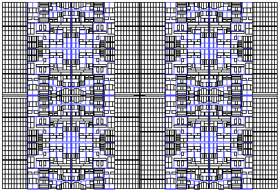
Sample 20 ands 14 nm Planar Layout Stress Test Cases
OAS = OASIS
GDS = GDSII
Workflow Auditor Point Tools
TM
®
© Getty Images
NEW at Yotta Data Sciences
* US Patents 9,122,825, 8,555,219, 8,266,571 and 7,685,545.
International Patents: China 200980129771.8, Japan 4768896, Korea 10-1580258, Israel 209907, European Patent 2310967.
© 2008-2024 Yotta Data Sciences, Inc. All rights reserved.
February 16, 2024- Yotta is offering, to qualified partners, a six-month evaluation-period, with support, for its SEMI P39-0416 OASIS Reader/Writer Source Code.
Visit Page: OAS Reader/Writer
Visit Page: OAS Source Code