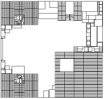
SIMULATED LARGE 20 nm SMART PHONE SoC STRESS TEST CASE

This 20 nm design simulates a large System on Chip (SoC), similar to a smart phone chip. It is 10164.1 microns wide and 9645.8 microns high. It features:
- 20 nm gate length; 64 nm SRAM metal pitch; 72 nm standard cell metal pitch
- two processor subsystems, each with an embedded processor core similar to an ARM processor and 6 MB of SRAM;
- two DSP processor subsystems, each with 1 MB of SRAM;
- a GPU subsystem with 16 MB of SRAM;
- numerous logic blocks around the perimeter of the design;
- a 58 million instance standard cell region in the center of the design; and
- polygons colored for double patterning on gate, contact, and metal layers.
The design has 30 MB of embedded SRAM plus cache and other embedded memory blocks, totaling 290 million SRAM bits including ECC. After hierarchy expansion there are about 92.7 million placed standard cell instances and about 2.57 billion transistors.
With little repetition outside of the SRAM areas, this design will stress the data size and single-block capacity of your tools. The preliminary version of the GDSII file is about 84.4 gigabytes in size; the OASIS file is about 4.4 gigabytes in size.


 | ||||

Typically, at each new generation of semiconductor technology design and semiconductor manufacturing tools do not perform well or not at all. Always, tool manufactrurers and siftware developers seek test cases from their customers that will take them a generation or so ahead. Such test cases are not available for a few reasons. First, they're not designed yet. Second, when they become available, they're considered proprietary.
Yotta developed simulated stress test cases that will mimic the physical layout of a commercial design without having to make them functional. The functionality of the design has less to do with the stressing of design and manufacturing tools than the amount, type and varied pattern density of the layout data.
typedef struct _oasisReaderPath {
oasisUInt layer,dataType,halfWidth;
oasisInt startExt,endExt;
rawPointList *ptList;
oasisPropertyList *propList;
} oasisReaderPath;
Production 20 nm Merchant Smart Phone Stress Test Case Data Sheet
Sample 20 ands 14 nm Planar Layout Stress Test Cases
OAS = OASIS
GDS = GDSII
Workflow Auditor Point Tools
TM
®
© Getty Images
NEW at Yotta Data Sciences
* US Patents 9,122,825, 8,555,219, 8,266,571 and 7,685,545.
International Patents: China 200980129771.8, Japan 4768896, Korea 10-1580258, Israel 209907, European Patent 2310967.
OASIS® is a Registered Trademark of Thomas Grebinski
© 2008-2024 Yotta Data Sciences, Inc. All rights reserved.
February 16, 2024- Yotta is offering, to qualified partners, a six-month evaluation-period, with support, for its SEMI P39-0416 OASIS Reader/Writer Source Code.
Visit Page: OAS Reader/Writer
Visit Page: OAS Source Code