


DESIGN AND MANUFACTURING LAYOUT STRESS TEST CASES


Since Moore's Law became the touchstone driving the advanced design and manufacture of integrated circuits, developers of the underlying technology have had to rely on a lot of guesswork about what it would mean to meet the next generations of the law. Even the scientists and engineers closest to the the history of the past technological successes really have not known enough to share, with confidence, what would be needed to automate the design and manufacturing processes the next time and the next.
Furthermore, whatever had been learned was held closely / not shared fully with outsiders even with those that were the most trusted. Whatever had been learned, though, was the past not necessarily projecting the future. As well, what was learned was pressed into production-worthy efforts, of the moment, and not efforts to help its partners automate what they had learned. Helping has always been viewed as a major, unproductive, distraction from getting chips out the door as soon as possible. Most important is that every successful company in this industry has never really known about what they've learned until the chips were shipped and in the products; functioning as well as they were able to make them function. Brute force effort, money and dogged persistence are what have driven this industry's successes; only knowing fully about what, actually, had worked after the fact.
The shift of power to the semiconductor industry's partners and their ability to anticipate and even drive the successes along with the dictates of the law has changed dramatically over the last decade. A farmer at the further reaches of the globe can easily gain access to a computational capability rivaling that used by those designing and making integrated circuits. Full chip layout design simulations, gigabytes in size, can be compiled and recompiled on a cloud server, such as Amazon's cloud server, from home enabling, anticipatory, options for design and manufacturing automation. Options that can be offered through brute-force simulations of next generation design and manufacturing layout geometry for dollars per month. The developing knowledge/understanding about how to handle design geometry this way, computationally, has outstripped the pace of Moore's Law. With this capability, the cost and the needed success to automate next generation design and manufacturing can be anticipated, honed and honed again and again, today, even before the next generation of chips are designed. Again, the cost . . . relatively nothing when compared to the costs needed to do so a decade ago.
Having access to such a computational capability opens up the mind of the user to more relevant matters such as, how will this type of next-generation design impact the performance of design and manufacturing automation technology which will play a critical role in bracketing a chip's time-to-market.
This is where Yotta has placed its efforts recently. It has developed a way to allow design and manufacturing automation companies to run simulations of what likely will be the computational load from likely integrated circuit designs that have yet to be designed. It has developed a full chip design layout generator/simulator that can offer layout designs approaching commercial grade. They can be used to develop next-generation design and automation technology that can handle the computational requirements for, as examples, 10 nm and 7 nm design layouts that are based on finFET manufacturing technology. Having the next-to-the-real-thing as design layouts allows the delivery of more profitable automation when and even long before the automation is needed.
Blockage mask, cut masks, diffraction gratings, triple-patterning, 1-D and 2-D layouts are just a few of the features we offer within our full-chip stress test case designs. Essentially, all of the features we offer can be mixed together to create a behavior, computationally, that aids with the development of highly advanced automation capability not achievable today by any other means.
Yotta is able to do this because of its deep working, hands-on, knowledge about the design and manufacture of next-generation integrated circuits. Yes, the computational capability is there to make something like this happen but, one needs this deep understanding as well. We've had our stress test cases compared to real designs. The differences are not easy to find. Our IP is real. How they are assembled to make phone chips, network processors (SoCs), CPU and SRAMs is real-world IP assembly. The floorplanning is real-world as well. There is no reason to think you'll need a on-the-floor chip design to develop your automation over what we're offering here today. In fact, you'll be hard pressed to find anyone who will be willing to share IP like this. Yotta believes that you will lose nothing and gain far more in your advanced automation capabilities by using its simulated stress test case designs.
On our site are many examples of what we can do and how we can work with you. There are many ways to contact us to start a conversation about your needs, specifically. At this time, we supply circuit simulations for planar and finFET manufacturing technology. The design rules can be set to be more or less aggressive. The layer mapping, number of layers, IP mix, etc. can easily be dialed in as well. All of this can be reviewed even before contacting us by downloading our data sheets and sample planar and finFET test cases. We'll be happy to discuss your needs.
Planar Layout Stress Test Cases
20 nm
14 nm
finFET Layout Stress Test Cases
10 nm
7 nm
Click . . . to explore.
{0|1} = Cut Mask
{0|1} = Blockage Mask
{0|1} = Diffraction Grating
{0|1} = Fin Pitch Doubling
0 = Not a variant
1 = Variant
| = or
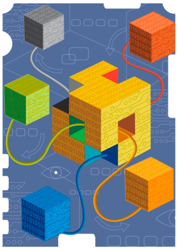
Developing Computationally Intensive, Production-worthy, Integrated Circuit Design and Manufacturing Automation Technology Ahead of the Curve ... Yotta's Stress Test Cases. Here is our mix of capabilities from IP that reflects the design of specific product types to various manufacturing techniques at all processing technology nodes. Yotta's Stress test case generator can virtually bring tomorrow's computational requirements for design and manufacturing automation today to those who need it for development today.
OAS = OASIS
GDS = GDSII
Workflow Auditor Point Tools
TM
®
© Getty Images
NEW at Yotta Data Sciences
* US Patents 9,122,825, 8,555,219, 8,266,571 and 7,685,545.
International Patents: China 200980129771.8, Japan 4768896, Korea 10-1580258, Israel 209907, European Patent 2310967.
OASIS® is a Registered Trademark of Thomas Grebinski
© 2008-2024 Yotta Data Sciences, Inc. All rights reserved.
February 16, 2024- Yotta is offering, to qualified partners, a six-month evaluation-period, with support, for its SEMI P39-0416 OASIS Reader/Writer Source Code.
Visit Page: OAS Reader/Writer
Visit Page: OAS Source Code